Semiconductor Fab Cleanroom
Overview
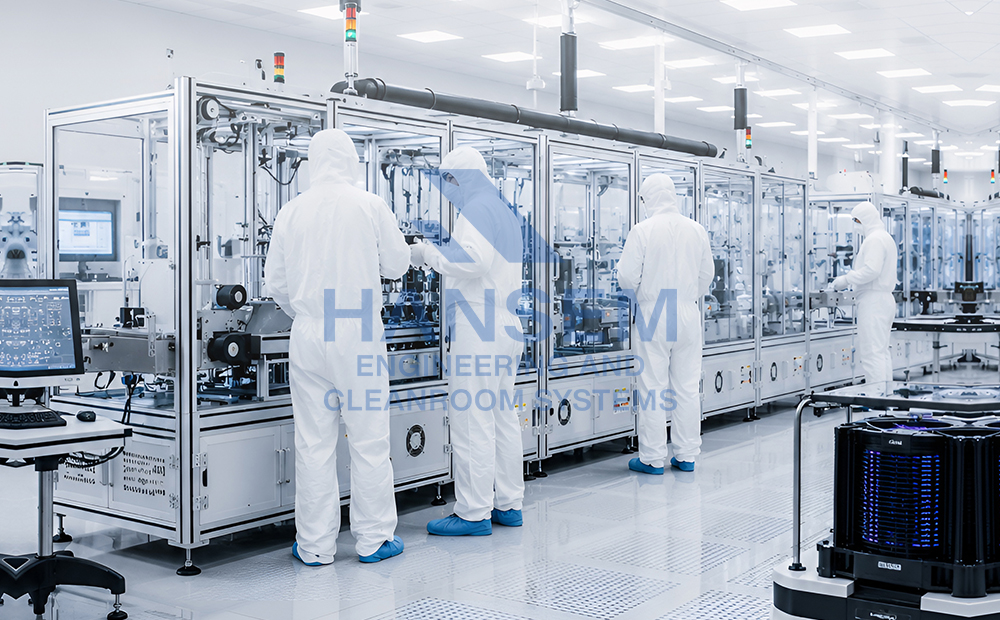
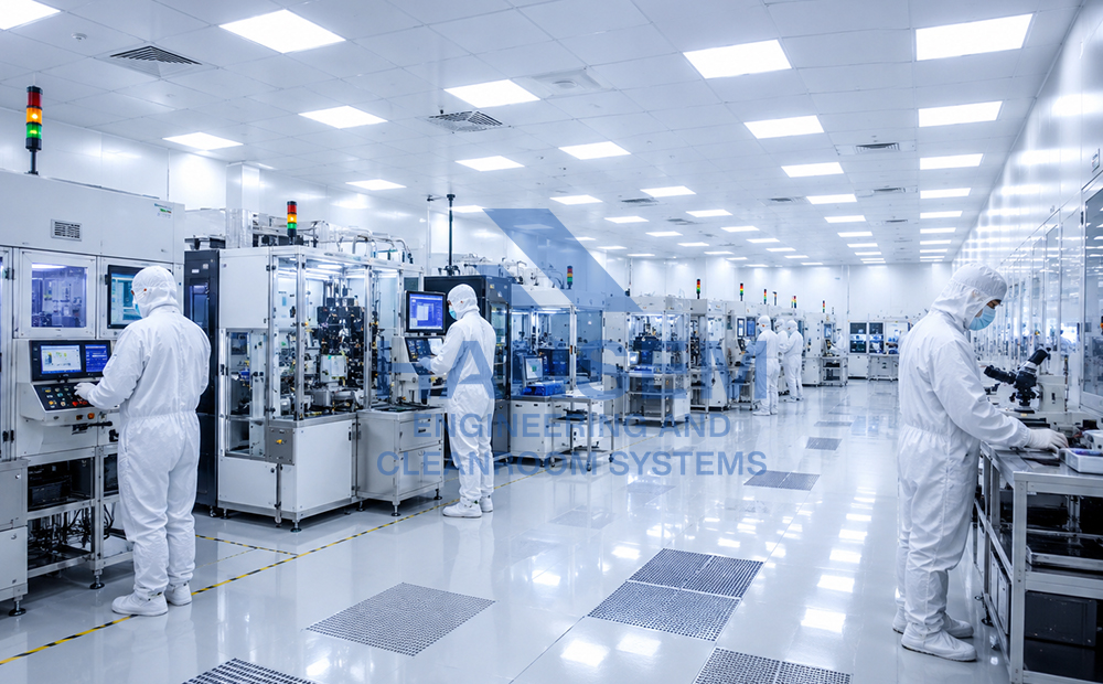
Semiconductor Fabrication Cleanrooms represent the highest standard of cleanroom engineering. Designed for wafer fabrication and advanced microelectronics manufacturing, these facilities maintain ultra-low particle concentrations with precise environmental control, vibration isolation, and stringent airborne molecular contamination (AMC) management.
Every aspect of the facility – from airflow and pressure control to filtration, temperature, humidity, electrostatic discharge (ESD), and chemical handling – is engineered to protect nanoscale manufacturing processes and maximize production yield.
Key Features
- ISO Class 1–5 environments
- Full ULPA filtration systems
- Vertical unidirectional airflow
- Fan Filter Unit (FFU) ceiling systems
- Raised perforated flooring
- AMC control
- ESD protection systems
- Vibration isolation
- Precision temperature control (±0.1–0.5°C)
- Precision humidity control (±1–3% RH)
- BMS & SCADA integration
- Real-time environmental monitoring
- High-reliability HVAC systems
- Redundant utilities and process support
Applications
- Wafer Fabrication
- Semiconductor Packaging
- MEMS Manufacturing
- Microelectronics
- Photonics
- Display Manufacturing
- AI Chip Production
- Power Semiconductor Manufacturing
- Advanced Packaging Facilities
International Design Standards
- ISO 14644 Cleanrooms
- EU GMP
- US FDA
- WHO GMP
- IEST Recommended Practices
- ASHRAE HVAC Standards
- SMACNA Standards
- SEMI Standards
- NFPA Fire Protection Standards